


英商劍橋氮化鎵器件有限公司
Cambridge GaN Devices
由英國劍橋大學分立出來的 Cambridge GaN Devices (簡稱 CGD),是一家無晶圓廠半導體公司,致力於開發一系列基於 GaN 的節能功率裝置,以實現更環保的電子產品。
業界首創、易於使用的增強模式 GaN
積體電路增強模式 GaN:具有最先進靜態和動態性能的新型平台,可增加內部閘極端子的易用性和智慧溫度控制,進而提高閘極可靠性。 與其他現有GaN 裝置不同,我們的智慧型 ICeGaN™ 電晶體可與標準矽閘極驅動器搭配工作,且無需負電壓關斷,因此不必配置外部、昂貴的驅動和箝位介面。最後GaN 功率電晶體的工作方式與 MOSFET 大致相同。
節能50% 以上
隨著全球電氣化快速發展,對高效和創新解決方案的需求也與日俱增。 與最先進的矽元件相比,ICeGaN™ 功率元件可在更高的開關頻率下工作,具有更低的損耗和導通電阻,還可提供更高性能,同時將節能效果提高 50%。
體積縮小至兩倍以上
GaN 電晶體可輕鬆地以更高頻率運行許多電路拓撲,同時仍能實現極高能效,從而使許多應用變得更小、更輕。CGD 的 ICeGaN™ 可將多個特性整合至增強型 GaN 電晶體,運行溫度更低,可靠性更高,與矽相比,GaN 具有可以實現前所未有的功率密度的優勢。


產品展示
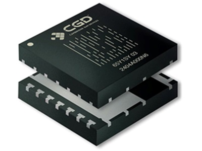
CGD65C055SP2
P2 series 650 V / 55 mΩ GaN HEMT with ICeGaN® Gate
CGD65C055SP2 is a 650 V power transistor utilising the superior material attributes of enhancement mode normally-off GaN-on-Si for high power applications, delivering high current, impressive breakdown voltage, and high switching frequency. Central to its design is CGD's hallmark ICeGaN® gate technology which provides a wide 9-20 V gate drive voltage, a 3 V threshold voltage, genuine 0 V turn off, and fast turn-on time for high frequency operation and easy paralleling. This ensures compatibility with almost all available Si/SiC MOSFET and IGBT gate drivers.
Presented in a thermally optimised compact 10x10 mm² SMD package with wettable flanks, this 55 mΩ GaN power transistor is tailored for bottom side cooling and superior thermal resistance, making it ideal for multi-kW applications with demanding performance criteria.
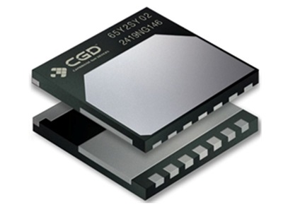
CGD65D055SP2
P2 series 650 V / 55 mΩ GaN HEMT with ICeGaN® Gate and Dual Gate Pinout
CGD65D055SP2 is a 650 V power transistor utilising the superior material attributes of enhancement mode normally-off GaN-on-Si for high power applications, delivering high current, impressive breakdown voltage, and high switching frequency. Central to its design is CGD's hallmark ICeGaN® gate technology which provides a wide 9-20 V gate drive voltage, a 3 V threshold voltage, genuine 0 V turn off, and fast turn-on time for high frequency operation and easy paralleling. This ensures compatibility with almost all available Si/SiC MOSFET and IGBT gate drivers.
The dual gate pinout design allows for easy paralleling and versatile PCB design. Presented in a thermally optimized 10x10 mm² SMD package with wettable flanks, this 25 mΩ GaN power transistor is optimized for dual side cooling and superior thermal resistance, making it ideal for multi-kW applications with demanding performance criteria.